
Short answer: wafer probe screens dies through their wafer-level contacts; final test checks packaged devices against an agreed production test program; bench validation investigates how first silicon behaves. They answer different questions. A small MPW project needs an agreed test route, not an assumption that “packaged” means “fully tested”.
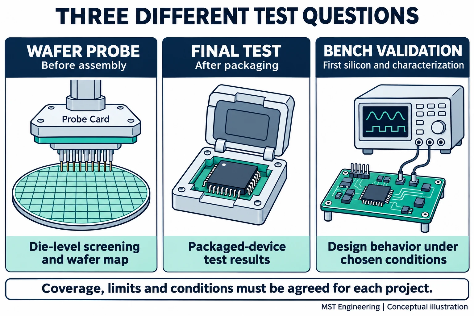
Illustration: MST Engineering, AI-generated conceptual diagram. The three panels compare scopes, not a mandatory sequence or an actual customer setup. The explanations below provide the text equivalent.
What does each test stage deliver?
| Scope | What is connected | Evidence to specify |
|---|---|---|
| Wafer probe / wafer sort / CP | Probes contact accessible die pads before the chosen assembly flow | Wafer/die identity, map orientation, measured results and bin definitions |
| Packaged-device final test / FT | A packaged IC connects through a socket or other test interface | Device identity, program revision, conditions, limits and pass/fail data |
| Bench validation / characterization | Samples operate on a measurement or evaluation setup | Setup and firmware revisions, measured behavior, conditions and unresolved issues |
Amkor lists wafer probe, package test and test development as separate services (https://amkor.com/test-services/) . UTAC also describes probe cards, load boards and test-program development (https://utacgroup.com/test-services/) . These are examples of industry service scopes, not confirmation that either company has accepted an MST project.
Does a small prototype run need wafer probe?
Resolve four questions with the design, assembly and test teams:
- What decision will the measurements support: reject dies before assembly, check packaged units, or investigate the design?
- Are the required signals accessible at wafer level, and are a compatible probe interface and test program available?
- Does the run return wafers, selected dies or already packaged samples? Who controls the wafer map and sample selection?
- What are the setup cost, schedule and risk of assembling unscreened dies compared with the proposed screening route?
Do not assume a prototype route must include every production stage. Equally, an assembly inspection does not establish electrical functionality. Record any omitted test and its consequence before ordering. UMC's testing service description illustrates why program development and probe hardware need their own preparation (https://www.umc.com/en/StaticPage/testing_services) .
Turn “please test the chips” into a usable test brief
Use one row per measurement. The following is an illustrative worksheet, not a universal test specification.
| Measurement | Inputs the design team must define | Requested record |
|---|---|---|
| Supply current | Rail names, power sequence, operating mode, temperature and limit | Measured value, units and device ID |
| Digital interface | Pin mapping, voltage levels, clock rate, firmware/vector revision and expected response | Result and failure log |
| Analog function | Stimulus, load, bandwidth, settling time, instrument method and limits | Raw readings and calculated result |
| Memory, if present | Address range, patterns, timing, programming conditions and acceptance rule | Tested region and failure information |
Assign an owner to the program, probe card/load board, socket, firmware and results review. Agree which tests run on every device and which characterization tests use selected samples. A device passing a limited screen has passed that screen under its stated conditions; this does not establish complete design validation or reliability qualification.
Compare test costs on the same basis
For budgeting, separate test development + test hardware + execution charges + agreed logistics. State whether execution is billed by engineering time, tester time or device count, and how retest is charged. The number tested is not automatically the number of passing deliverable chips. Use the MPW quotation-scope worksheet (https://store.mst-sg.com/community/t/32-comparing-mpw-quotations-normalize-fabrication-packaging-and) to align the rest of the project.
Where physical products enter the plan
- IC test sockets (https://store.mst-sg.com/store/ic-test-sockets) connect packaged devices. Match the controlled outline, contacts, pin map and electrical/thermal requirements; a socket alone does not supply a test program.
- Empty IC packages (https://store.mst-sg.com/store/empty-ic-packages) need a die-attach and bonding review. They are not finished ICs.
- Gel carrier boxes (https://store.mst-sg.com/store/gel-carrier-boxes) support handling. Select usable area, clearance and retention method for the actual die and transport process.
For the assembly handoff, continue with the bare-die-to-sample guide (https://store.mst-sg.com/community/t/34-from-mpw-bare-die-to-qfn-samples-package-fit-sample) . To discuss a project, email [email protected] or use the MPW enquiry (https://store.mst-sg.com/mpw#mpw-inquiry-form) with a non-confidential scope summary. Arrange the NDA and secure exchange before sending design files.
Questions behind this guide
Public discussions ask how analog IC testing and validation differ (https://www.reddit.com/r/chipdesign/comments/1ezxpen/) and what follows tapeout (https://www.reddit.com/r/chipdesign/comments/11dgs2o/tapeout/) . They inform the question selection; the technical explanation above is MST's original synthesis using the primary references linked in the text. Reviewed 2026-11-12.