
Receiving bare dies is only one step toward measuring your first silicon. Before layout is frozen, connect the die outline and pad map to an assembly drawing, a package interface and a test plan. This guide uses a nominal QFN area check and a sample-allocation exercise to show what must still be confirmed.
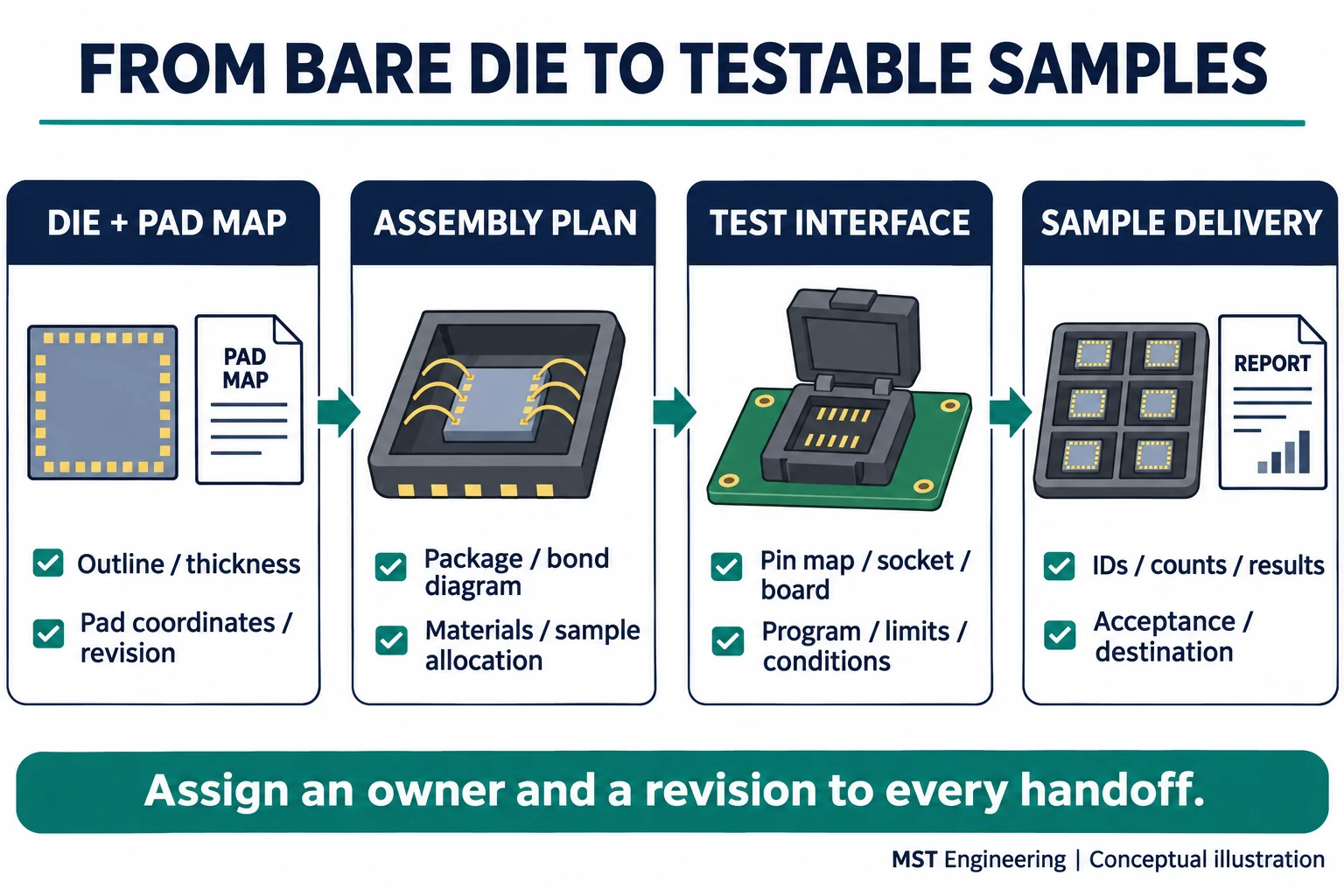
Illustration: MST Engineering, AI-generated conceptual diagram. Each handoff needs an identified owner and controlled revision; the drawing does not confirm a particular package or test route.
Before approving assembly, agree whether the requested measurements belong to wafer probe, packaged-device final test or bench validation. The test-scope checklist (https://store.mst-sg.com/community/t/39-wafer-probe-final-test-or-bench-validation-a-test-scope) includes a test-brief worksheet. If samples will be shipped as bare die, review the usable area, clearance and retention method of the gel carrier box (https://store.mst-sg.com/store/gel-carrier-boxes) against the actual die and transport process.
Start from the measurement and work back to the package
List the signals, supplies, grounds, temperatures and measurements required for the first experiment. Decide how the die will connect to the instrument or board. An open-cavity package can be a candidate for some prototypes, but the package outline or connection count alone does not establish assembly suitability.
| Interface | Information to exchange with the responsible team |
|---|---|
| Die to attach surface | Die outline/thickness, usable attach area, adhesive, placement tolerance and backside requirements |
| Pads to package | Pad map/pitch/metallurgy, bond-finger layout, wire material/loop envelope and net mapping |
| Package to board/socket | Controlled outline drawing, terminal geometry, tolerances, exposed pad and orientation |
| Thermal/mechanical setup | Power, operating temperature, lid/cavity access, contact clearance and fixture constraints |
| Test to acceptance | Measurements, limits, program/board owner, data format and failure disposition |
Ask the assembly and test providers which drawing revisions they are reviewing. Two packages described as QFN48 can still require different sockets, boards or thermal interfaces. Do not approve a socket on the basis of pin count alone.
Worked example: nominal area is only the first screen
The Store listing for ALNP-48-7-5 (https://store.mst-sg.com/store/empty-ic-packages/ALNP-48-7-5) gives a nominal 5.2 mm × 5.2 mm die-attach area. For an invented square die of 3.0 mm × 3.0 mm, a centered area calculation leaves (5.2 − 3.0) / 2 = 1.1 mm on each side.
That is an arithmetic screen using the listed nominal area, not a qualification of this die/package combination. It does not prove adhesive fillet clearance, placement tolerance, access to bond fingers, acceptable wire loops, electrical performance or thermal compatibility. Confirm the current controlled drawing and assembly rules before selecting the package. A positive area margin cannot replace that review.
The open-cavity die-fit walkthrough (https://store.mst-sg.com/community/t/27-open-cavity-qfn-die-fit-check-step-by-step-die-attach-area) and QFN socket buying guide (https://store.mst-sg.com/buying-guides/qfn-test-socket-guide) provide related selection context. Treat dimensions as inputs to an engineering review, not a universal fit guarantee.
Allocate samples before promising a test quantity
In an invented planning exercise, 20 incoming dies are allocated as 2 for incoming inspection, 2 retained for investigation and 16 for assembly: 2 + 2 + 16 = 20. This is an allocation example, not a predicted yield. The inspection method may be destructive or non-destructive; agree its purpose and disposition with the provider.
Receiving 20 dies does not guarantee 20 passing packaged chips. Assembly loss, electrical failures, retest and failure analysis can affect the number available for the experiment. Define whether delivered quantities refer to untested dies, screened dies or samples passing specified tests. Agree how reserves and rejected parts are handled rather than assuming every received die can be used on the board.
Prepare a handoff that another team can execute
Create a shared checklist containing the die/pad-map revision, package/assembly drawing revision, material and wire requirements, sample allocation, inspection/test limits, fixture/board readiness and delivery destination. Assign a person responsible for each missing item.
The package and assembly selector (https://mst-sg.com/tools/package-selector/) helps organize candidates and constraints. The MPW sample-handling category (https://store.mst-sg.com/store/mpw-sample-handling) covers handling-related products; listing a product does not establish availability or compatibility for your project. Request confirmation against the actual requirements.
Primary references and further reading
- ALNP-48-7-5 Store listing (https://store.mst-sg.com/store/empty-ic-packages/ALNP-48-7-5) : nominal area used in the arithmetic example; request the current controlled drawing.
- MST packaging, wafer probe and test guide (https://mst-sg.com/news/mpw-packaging-wafer-probe-test/) : planning assembly and measurements before tapeout.
- MST MPW handoff handbook (https://mst-sg.com/tools/mpw-handoff-handbook/) : synthetic exercises for organizing delivery evidence.
Next step: request an MPW packaging and test scope review (https://store.mst-sg.com/mpw#mpw-inquiry-form) with a non-confidential die-size estimate, sample target and measurement needs. Use the MPW community (https://store.mst-sg.com/community/c/mpw) for general preparation questions; arrange secure transfer for restricted drawings or design files.
Catalog parts in this guide